
CVD (chemical vapor deposition) and a number of derived vapor phase deposition methods rely on a carrier gas transporting thermally sublimed species to a substrate on which films of semiconductors, metals or dielectrics are formed. Inherent advantages are a precise control of material fluxes and deposition conditions as well as the option to form sharp heterostructures, to achieve conformal coating and to easily scale-up the substrate area. These characteristics have made CVD methods commercially successful in a wide field of applications from advanced coatings / barriers to semiconductor electronics.
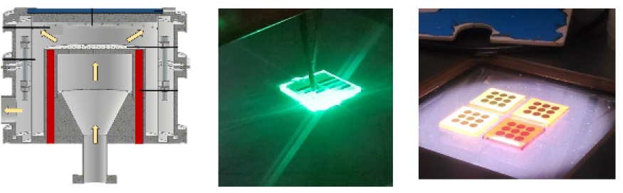
At CST, we are studying several of these processes like MOCVD, OVPD, PVPD, ALD, PECVD and CVD. A recent example is CVD of inorganic and hybrid organic inorganic trihalide perovskites, which constitute a fascinating class of materials especially for optoelectronic applications. As dedicated perovskite deposition tools were not available, let alone a known CVD synthesis route, we have successfully developed several prototype CVD test tools, including a large-area (12 cm × 8 cm substrate size) showerhead reactor (see above) and demonstrated light emitting diodes as well as photovoltaic cells processed on our CVD perovskite films. Current research is focused on understanding and improving the gas phase synthesis of perovskite materials and on studying the interrelation between material properties and device performance.
Detailed information on Novel CVD Technology can be found on the Projectwebsite