
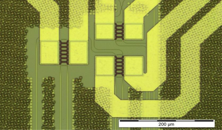
Project “SiGeSn laser for silicon photonics” (DFG 299480227): Current silicon-on-insulator technology allows monolithic integration of all key components other than the light source. Semiconductor lasers require a direct bandgap material that has to be provided via heterogeneous (wafer bonding) or hybrid (co-packing) integration. While direct growth of III-V materials on silicon has made rapid progress in recent years, it remains hindered by contamination issues or issues related to growth such as the difficulty of preventing the emergence of anti-phase domains. Direct growth of a group IV direct bandgap semiconductor onto silicon would enable further increase of the integration density and further cost reduction, allowing optical interconnects to be used at even smaller architectural levels such as at the chip-to-chip or intra-chip level, as well as mass-market optical sensor systems. At high enough Sn content, the GeSn alloy provides exactly this capability. Even though it remains a challenging material to grow and progress remains to be made in regards to defectivity and increased Sn content, rapid progress has been made in the last few years with continuous wave lasing, near-room temperature lasing and electrically pumped lasing having each been independently shown. Current work targets a combination of these characteristics, towards a practical, continuously operated and electrically pumped room temperature laser. To this end, we are exploring advanced strain engineering of SiGeSn multi-quantum well gain materials.
Project partners: Forschungszentrum Jülich, University of Stuttgart, Leibniz Institute for Innovative Microelectronics (IHP).
Detailed information on SiGeSn laser for silicon photonics can be found on the Projectwebsite